
The Role of PCB Stack-up in High-Frequency Applications
As electronic systems evolve, especially in telecommunications, aerospace, and high-speed computing, the demand for high-frequency signal transmission continues to rise. In these applications, the Printed Circuit Board (PCB) stack-up plays a critical role in determining performance, reliability, and signal integrity. Proper stack-up design can significantly mitigate signal loss, electromagnetic interference (EMI), and impedance mismatches—crucial considerations when operating at high frequencies.
What is a PCB Stack-up?
A PCB stack-up refers to the arrangement of conductive and insulating layers within a PCB. It defines how signal layers (where traces run) and plane layers (ground or power) are distributed across the board. In high-frequency designs, this configuration becomes a strategic element, influencing key electrical parameters and physical durability.
Why Stack-up Matters in High-Frequency Applications
At high frequencies—typically above 100 MHz and especially in the GHz range—signal wavelengths shorten, making PCBs more susceptible to:
· Signal attenuation
· Crosstalk
· Reflections and ringing
· Radiated emissions (EMI)
· Timing errors
A carefully designed stack-up helps mitigate these issues by:
1. Controlling Impedance: Differential and single-ended impedance must be tightly controlled to ensure signal integrity. Stack-up impacts trace width, spacing, and dielectric thickness—all critical in impedance tuning.
2.Reducing EMI: High-frequency signals can behave like radio waves, radiating from traces and causing interference. Strategic placement of ground planes in the stack-up can act as shields, containing these emissions.
3. Minimizing Crosstalk: Adjacent signal layers can interfere with each other. Proper layer sequencing and spacing in the stack-up reduce this risk.4. Enhancing Signal Return Paths: Return current tends to flow directly beneath the signal trace on the closest reference plane. A poor stack-up can force this current to take longer paths, introducing noise and increasing the risk of signal distortion.
What Makes Stack-Up Design Critical?
At high frequencies, signals behave less like simple voltage changes and more like electromagnetic waves. This makes them sensitive to impedance variations, layer transitions, and dielectric inconsistencies. A well-planned stack-up ensures:
· Stable impedance
· Minimized signal degradation
· Controlled EMI/RFI
· Reduced signal skew and reflections
· Optimal mechanical reliability
Key Elements of Stack-Up
1. Number of Layers
Choosing the number of layers is the first step in stack-up planning. More layers provide better isolation of signals and power/ground planes but increase cost and complexity. High-speed designs typically use 4, 6, 8, or more layers.
2. Layer Functions
· Signal Layers: Carry high-speed and low-speed traces.
· Plane Layers: Power (VCC, 3.3V, etc.) and Ground (GND) planes provide current return paths and EMI shielding.
· Mixed Layers: Occasionally, layers may carry both signals and power, though this is less ideal in high-frequency boards.
3. Dielectric Material
The material between copper layers determines the board's dielectric constant (Dk), loss tangent (Df), and signal speed. Common materials:
Material | Dk (Typical) | Df (Loss) | Comments |
FR-4 | ~4.2 | 0.020 | Standard, not ideal above 1 GHz |
Rogers 4350 | ~3.48 | 0.0037 | Excellent for RF and microwave |
Isola 370HR | ~3.8 | 0.005 | High-speed digital compatible |
Nelco N4000 | ~3.7 | 0.006 | Good thermal and electrical properties |
High-frequency PCBs benefit from low-Dk and low-Df materials to reduce signal loss and propagation delay.
4. Trace Impedance Control
The characteristic impedance of a trace is a function of:
· Trace width
· Dielectric height
· Copper thickness
· Dielectric constant (Dk)
Controlled impedance (typically 50Ω single-ended or 100Ω differential) is vital for signal integrity. Stack-up helps set the right spacing and material thickness to meet these values.
8-Layer Stack-Up (Advanced High-Frequency)
| L1 | Signal (High-Speed) | | L2 | Ground Plane | | L3 | Signal (Control/Data) | | L4 | Power Plane | | L5 | Ground Plane | | L6 | Signal (Clock/Data) | | L7 | Ground Plane | | L8 | Signal (High-Speed) |
· Ideal for complex systems with multiple interfaces (USB 3.0, DDR4, RF)
· Redundant ground layers enhance shielding and return paths
Advanced Tips for High-Frequency Stack-Up
· Minimize Layer Changes for High-Speed Nets: Each via adds impedance discontinuity; avoid unnecessary layer transitions.
· Backdrilling Vias: Removes unused stub portions in plated-through-hole (PTH) vias to prevent reflections.
· Use Differential Pairs Wisely: High-speed signals like USB, HDMI, and LVDS need tightly coupled differential pairs with matched lengths and spacing.
· Keep Traces Short and Direct: Longer traces act like antennas; short, matched routes are essential.
· Use Stitching Vias: Connect adjacent ground planes with stitching vias to provide continuous return paths and minimize ground bounce.
Best Practices for High-Frequency Stack-up Design
- Use Ground Planes Wisely:
· Place continuous ground planes adjacent to signal layers to maintain consistent return paths.
· Avoid breaks or splits in ground planes.
- Symmetrical Layering:
· Maintain symmetry in the stack-up to prevent mechanical stress and warping, which can affect high-speed performance.
- Dielectric Selection:
· Choose low-loss dielectric materials like Rogers, Nelco, or Isola, which maintain stable dielectric constants (Dk) at high frequencies.
- Impedance Matching:
· Use field solvers and simulation tools to calculate and verify impedance across all signal traces.
· Stack-up should be designed with the trace geometry that meets the required impedance.
- Controlled Trace Routing:
· Keep high-frequency signals on internal layers sandwiched between ground planes to minimize radiation and external noise pickup.
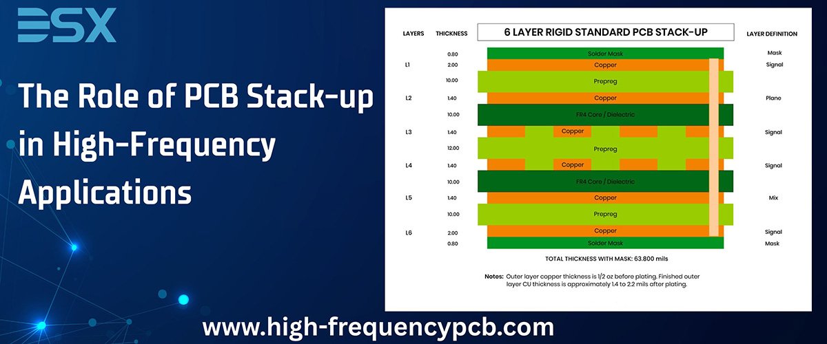
Example of a 6-Layer Stack-up for High-Frequency Use
Layer | Description |
L1 | Signal (High-speed) |
L2 | Ground Plane |
L3 | Signal (Low-speed/Control) |
L4 | Power Plane |
L5 | Ground Plane |
L6 | Signal (High-speed) |
This type of stack-up allows high-speed signals to be routed close to reference planes, reducing loop area and EMI, while also separating noisy power planes from sensitive signals.
In high-frequency PCB applications, stack-up design is more than just a structural decision—it's a cornerstone of electromagnetic performance. A thoughtful stack-up can be the difference between a robust, high-performing system and one plagued by signal integrity issues. As frequencies climb, investing time and simulation resources into stack-up planning becomes indispensable for success.
The Role of PCB Stack-up in Hi
 Why Are High-Frequency PCBs Es
 High-Frequency PCB vs. RF PCB:
 Why Signal Integrity Matters i